
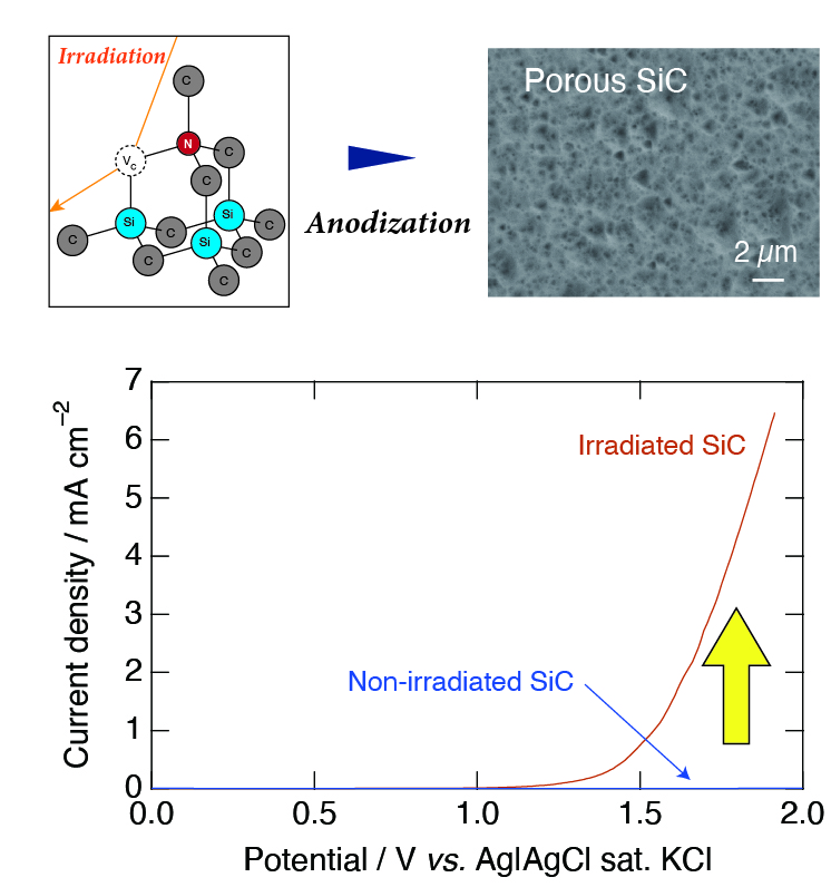
 By using metal or semiconductor materials as electrodes, the nanofabrication of such materials is achieved by anodization. We conduct applied research on the fabrication of nanoporous materials such as silicon (Si), silicon carbide (SiC), and diamond nanoporous based on anodization. In addition, the production of nanostructures of metals is studied using these nanoporous materials as templates.
Since SiC and diamond are mechanically and chemically stable, it is well-accepted that the surface processing of SiC and diamond is difficult. We have realized the surface processing based on anodization by generating point defects and stacking faults in the desired locations of these semiconductor materials using high-energy ion irradiation or mid-infrared free electron laser irradiation technologies.
Related publications
・ The Journal of Physical Chemistry C 2020, 124, 11032-11039.
・ The Journal of Physical Chemistry Letters 2022, 13, 2956-2962.
・ Electrochemistry Communications 2023, 149, 107473.
2. Metal nanostructure formation using anodic porous silicon
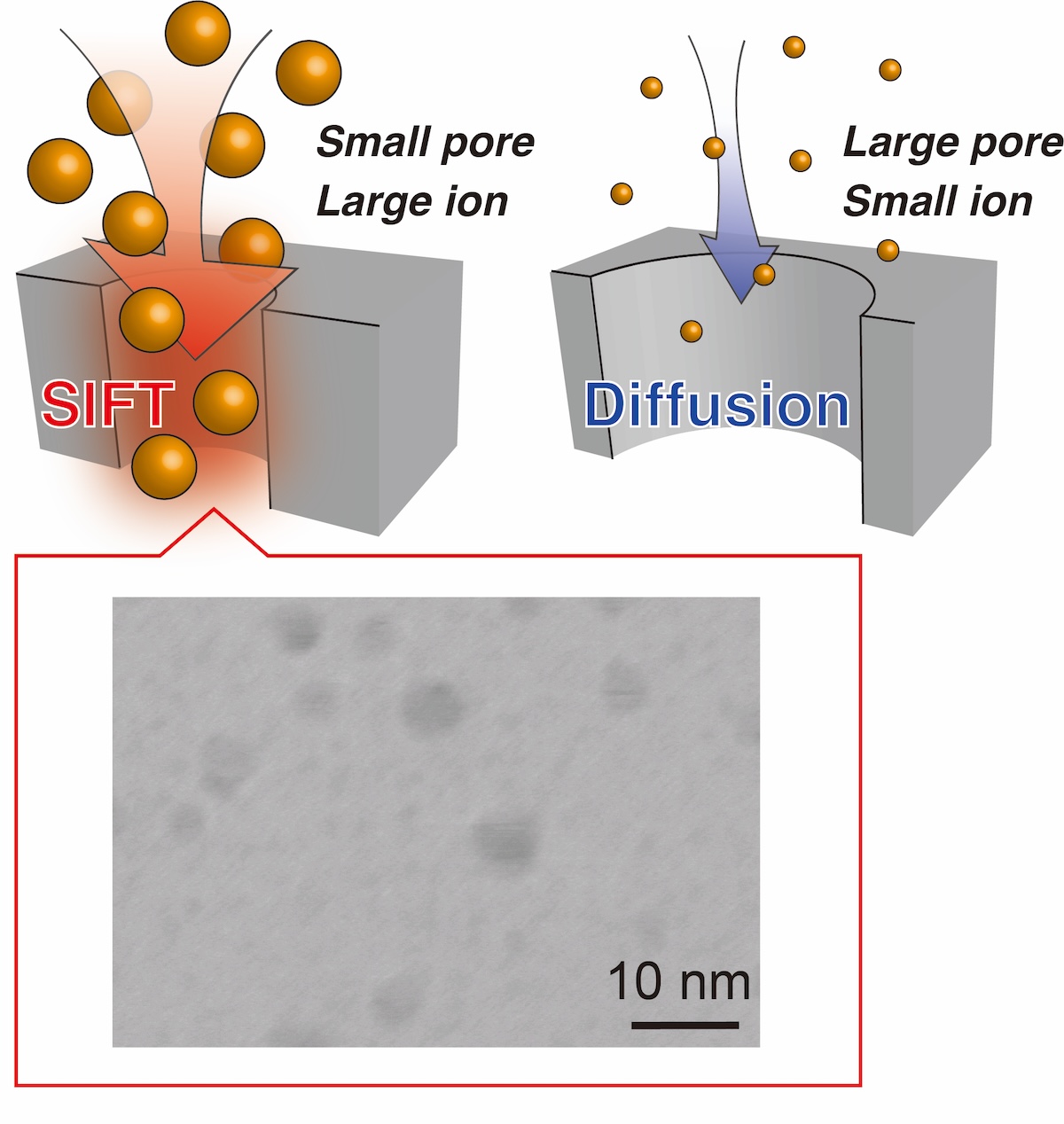 Nanoporous silicon produced by anodization can be used as template electrodes for electrochemical reactions, making it possible to form fine nanostructures such as metal nanoparticles and nanorods. However, the narrow cavity of nanopores strongly restricts the diffusion of metal ions, which are the precursors for producing metal nanoparticles and nanorods, in aqueous solutions, and in many cases, it is very difficult to make the reduction reaction proceed so that the pores fill up.
We have developed a method to drastically accelerate the transfer of metal ions in nanopores by actively designing the hydration interactions between the surface and ions. This method provides an abundant supply of metal ions even in extremely narrow cavities such as 2~3 nm in diameter, and we have shown that it is possible to mass-produce metal nanoparticles in a short period of time within nanoporous silicon electrodes.
Related publications
・ Chemical Physics Letters 2012, 542, 99-105.
・ The Journal of Physical Chemistry C 2015, 119, 19105-19116.
・ The Journal of Physical Chemistry C 2016, 120, 24112-24120.
3. Chemical dicing of silicon using graphene nanoribbons
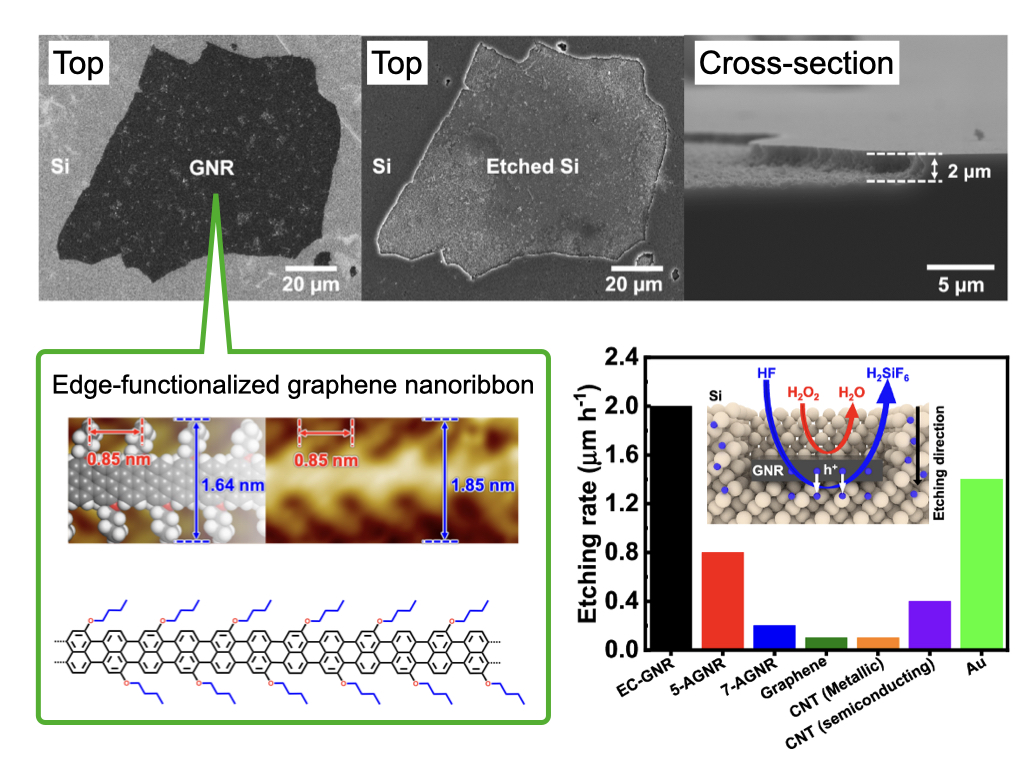 Semiconductors like Si (silicon) are cut from wafers and used for device fabrication. In this process, it is common to use a method called dicing. During dicing, waste dust is generated, and the smaller the cutting size, the more Si is wasted as dust.
We are advancing the development of a chemical dicing method using a carbon catalyst, which generates almost no waste dust. In general, carbon is not known for its catalytic performance, and it was not expected to be effective as a catalyst for Si chemical dicing. However, in collaboration with our research partners, we have successfully designed the world’s most active carbon catalyst for chemical dicing by using a new carbon material, graphene nanoribbons, as the catalyst.
Related publications
・ Nature Communications 2024, 15, 5972.
・ The Journal of Physical Chemistry C 2025, accepted for publication (DOI: 10.1021/acs.jpcc.4c08572).
4. Wet-electrochemical production of thin films of multicomponent alloys
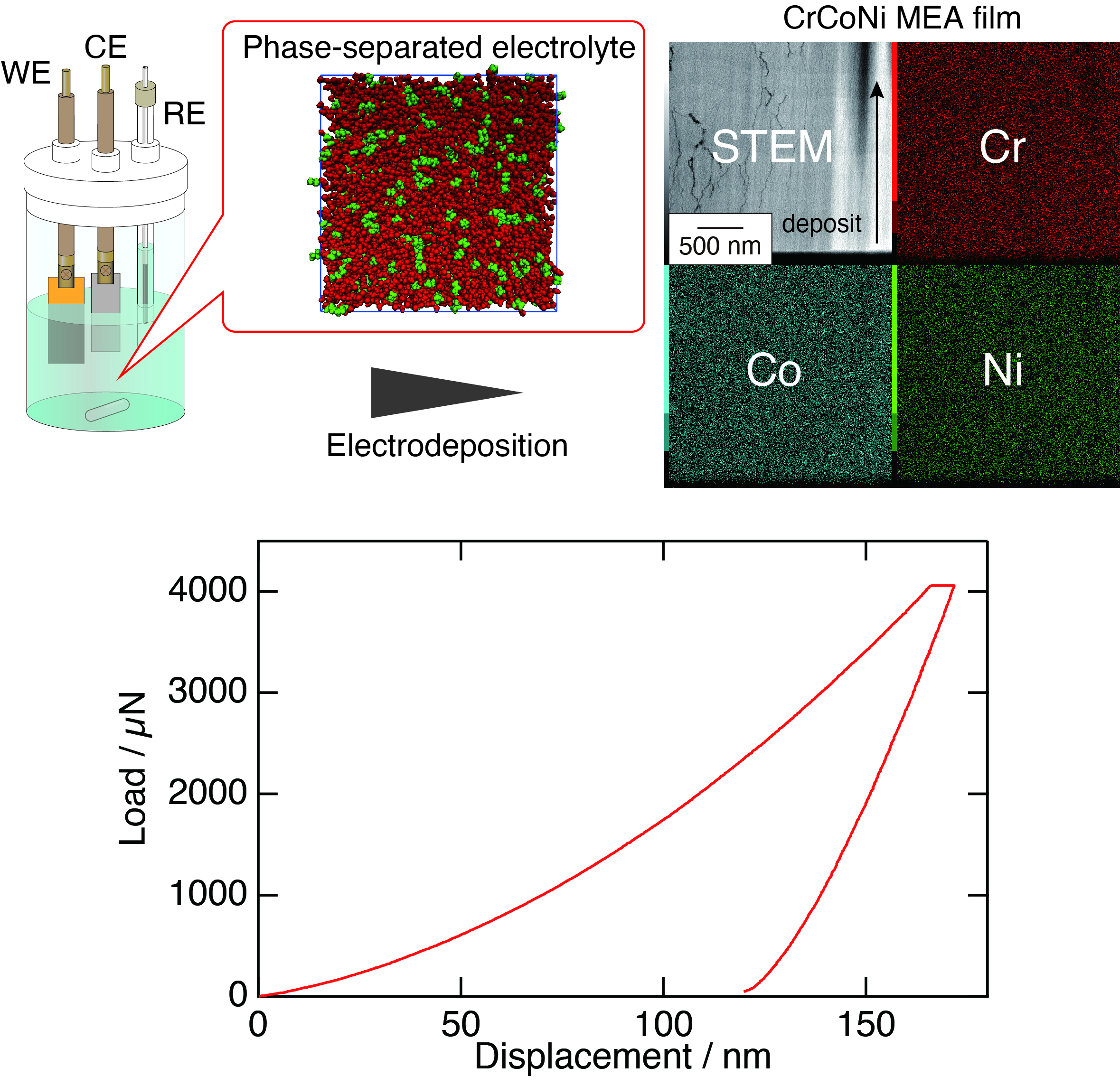 High-entropy alloys are known to exhibit an excellent balance of strength and toughness in bulk material research, and this property is also highly interesting for wear-resistant coatings. However, surfaces requiring wear resistance typically have three-dimensional complex shapes, and until now, no method has been reported to uniformly deposit high-entropy alloys on such materials. Electroplating is one of the few methods that can uniformly coat complex shapes; however, from both a thermodynamic and kinetic perspective, electroplating high-entropy alloys was considered difficult.
We have succeeded in creating Cr-Co-Ni medium-entropy alloy coatings with superior wear resistance and corrosion resistance, surpassing conventional hard chrome plating, by using a microphase-separated liquid, such as an emulsion, as the electrolytic solution. Currently, we are conducting research to design even better wear resistance by precisely controlling the constituent elements and composition. Additionally, we are also challenging the development of catalysts using relatively inexpensive 3d transition metal-based multi-component alloys.
Related publications
・ Electrochemistry Communications 2021, 128, 107057.
・ The Journal of Physical Chemistry C 2023, 127, 4696-4703.
・ Advanced Functional Materials 2025, 35, 2418621.
5. Production of helical nanostructures of metals and alloys
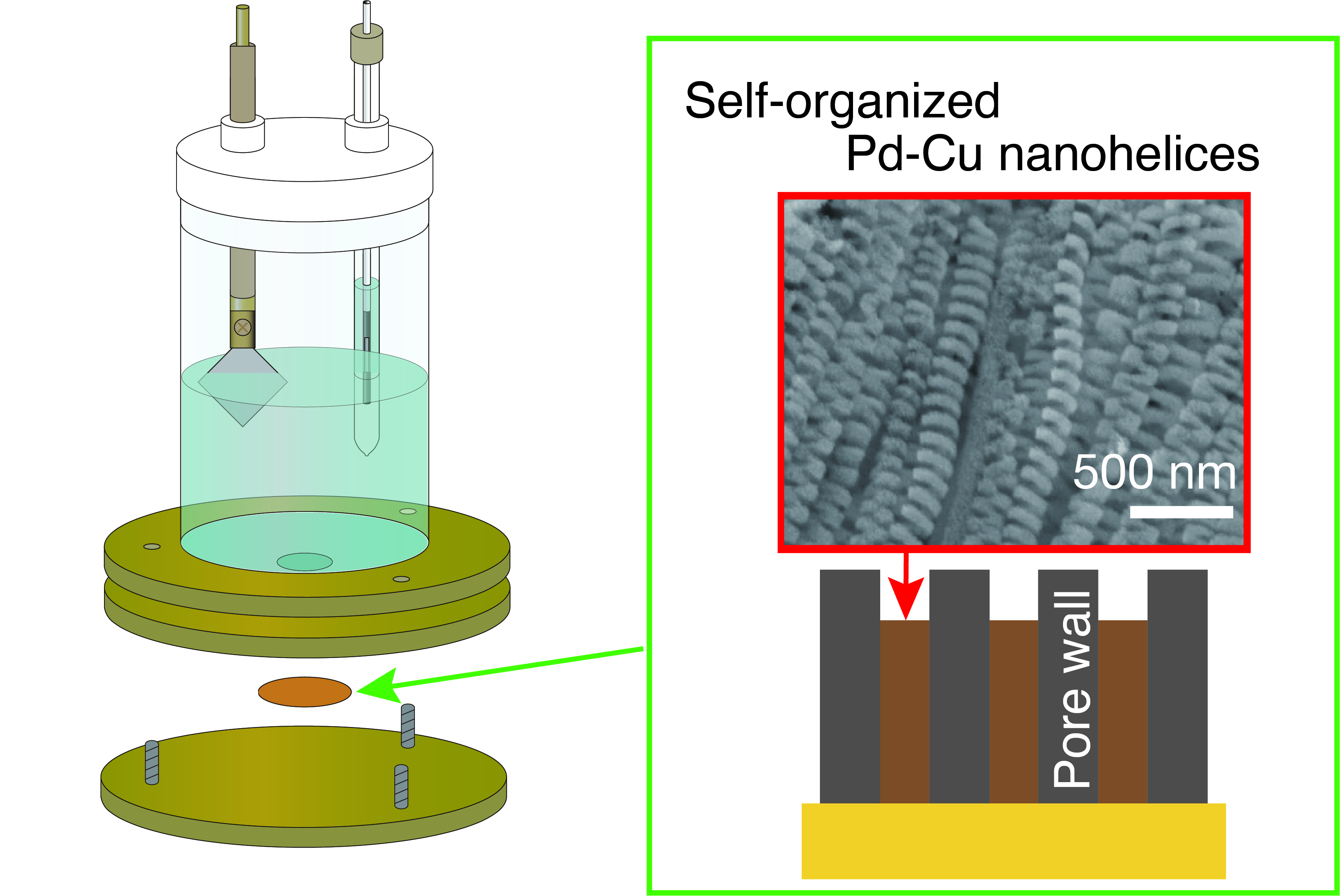 Materials with helical structures at the nanoscale do not allow mirror-image counterparts to overlap. This property is called chirality, and nanohelical materials can be considered a type of chiral material. Nanohelical materials made of metals, alloys, and semiconductors are expected to enable control of circularly polarized light. However, methods for precisely and efficiently fabricating large quantities of highly complex helical structures at the nanoscale have rarely been reported.
We have successfully enabled the fabrication of metal nanohelical structures and nanohelical pores on semiconductor wafers by precisely designing a self-organization process in the reduction deposition of metals via wet processing. This approach is expected to pave the way for the development of new chiral materials science for metals and semiconductors.
Related publications
・ ACS Applied Materials & Interfaces 2019, 11, 48604-48611.
・ Electrochemistry Communications 2020, 114, 106714.
・ Nano Letters 2023, 23, 462-468.